© by Tony van Roon
The
555 timer IC was first introduced around 1971 by the Signetics Corporation as
the SE555/NE555 and was called "The IC Time Machine" and was also the
very first and only commercial timer ic available. It provided circuit designers
and hobby tinkerers with a relatively cheap, stable, and user-friendly
integrated circuit for both monostable and astable applications. Since this
device was first made commercially available, a myrad of novel and unique
circuits have been developed and presented in several trade, professional, and
hobby publications. The past ten years some manufacturers stopped making these
timers because of competition or other reasons. Yet other companies, like NTE (a subdivision of Philips) picked up where
some left off.
This primer is about this fantastic timer which is after 30 years
still very popular and used in many schematics. Although these days the CMOS
version of this IC, like the Motorola
MC1455, is mostly used, the regular type is still available, however there have
been many improvements and variations in the circuitry. But all types are
pin-for-pin plug compatible. Myself, every time I see this 555 timer used in
advanced and high-tech electronic circuits, I'm amazed. It is just
incredible.
In this tutorial I will show you what exactly the 555 timer is and
how to properly use it by itself or in combination with other solid state
devices without the requirement of an engineering degree. This timer uses a maze
of transistors, diodes and resistors and for this complex reason I will use a
more simplified (but accurate) block diagram to explain the internal
organizations of the 555. So, lets start slowly and build it up from
there.
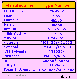
The first type-number, in Table 1 on the left,
represents the type which was/is preferred for military applications which have
somewhat improved electrical and thermal characteristics over their commercial
counterparts, but also a bit more expensive, and usually metal-can or ceramic
casing. This is analogous to the 5400/7400 series convention for TTL integrated
circuits.

The 555, in fig. 1 and fig. 2 above, come in two
packages, either the round metal-can called the 'T' package or the more familiar
8-pin DIP 'V' package. About 20-years ago the metal-can type was pretty much the
standard (SE/NE types). The 556 timer is a dual 555 version and comes in a
14-pin DIP package, the 558 is a quad version with four 555's also in a 14 pin
DIP case.
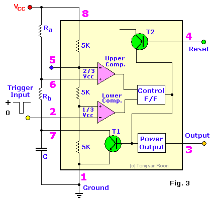
I nside the 555 timer, at fig. 3, are the
equivalent of over 20 transistors, 15 resistors, and 2 diodes, depending of the
manufacturer. The equivalent circuit, in block diagram, providing the functions
of control, triggering, level sensing or comparison, discharge, and power
output. Some of the more attractive features of the 555 timer are: Supply
voltage between 4.5 and 18 volt, supply current 3 to 6 mA, and a Rise/Fall time
of 100 nSec. It can also withstand quite a bit of abuse.
The
Threshold current determine the maximum value of Ra + Rb. For 15 volt operation
the maximum total resistance for R (Ra +Rb) is 20
Mega-ohm.
The supply current, when the output is 'high', is typically 1
milli-amp (mA) or less. The initial monostable timing accuracy is typically
within 1% of its calculated value, and exhibits negligible (0.1%/V) drift with
supply voltage. Thus long-term supply variations can be ignored, and the
temperature variation is only 50ppm/°C (0.005%/°C).
All IC
timers rely upon an external capacitor to determine the off-on time intervals of
the output pulses. As you recall from your study of basic electronics, it takes
a finite period of time for a capacitor (C) to charge or discharge through a
resistor (R). Those times are clearly defined and can be calculated given the
values of resistance and capacitance.
The basic RC charging circuit is shown in fig. 4. Assume that the
capacitor is initially discharged. When the switch is closed, the capacitor
begins to charge through the resistor. The voltage across the capacitor rises
from zero up to the value of the applied DC voltage. The charge curve for the
circuit is shown in fig. 6. The time that it takes for the capacitor to charge
to 63.7% of the applied voltage is known as the time constant (t). That time can
be calculated with the simple expression:
t = R X C
Assume a
resistor value of 1 MegaOhm and a capacitor value of 1uF (micro-Farad). The time
constant in that case is:
t = 1,000,000 X 0.000001 = 1
second
Assume further that the applied voltage is 6 volts.
That means that it will take one time constant for the voltage across the
capacitor to reach 63.2% of the applied voltage. Therefore, the capacitor
charges to approximately 3.8 volts in one second.
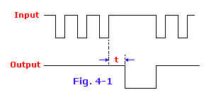
Fig. 4-1, Change in the input
pulse frequency allows completion of the timing cycle. As a general rule, the
monostable 'ON' time is set approximately 1/3 longer than the expected time
between triggering pulses. Such a circuit is also known as a 'Missing Pulse
Detector'.
Looking
at the curve in fig. 6. you can see that it takes approximately 5 complete time
constants for the capacitor to charge to almost the applied voltage. It would
take about 5 seconds for the voltage on the capacitor to rise to approximately
the full 6-volts.
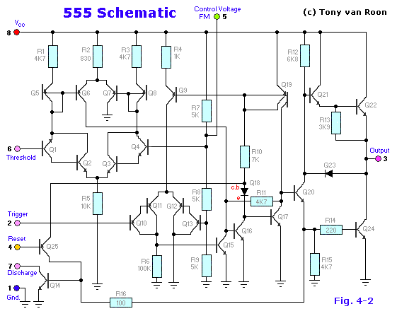
Definition of Pin Functions:
Refer to the
internal 555 schematic of Fig. 4-2
Pin 1
(Ground): The ground (or common) pin is the most-negative
supply potential of the device, which is normally connected to circuit common
(ground) when operated from positive supply voltages.
Pin 2 (Trigger): This pin is the input to the
lower comparator and is used to set the latch, which in turn causes the output
to go high. This is the beginning of the timing sequence in monostable
operation. Triggering is accomplished by taking the pin from above to below a
voltage level of 1/3 V+ (or, in general, one-half the voltage appearing at pin
5). The action of the trigger input is level-sensitive, allowing slow
rate-of-change waveforms, as well as pulses, to be used as trigger sources. The
trigger pulse must be of shorter duration than the time interval determined by
the external R and C. If this pin is held low longer than that, the output will
remain high until the trigger input is driven high again. One precaution that
should be observed with the trigger input signal is that it must not remain
lower than 1/3 V+ for a period of time longer than the timing cycle. If
this is allowed to happen, the timer will re-trigger itself upon termination of
the first output pulse. Thus, when the timer is driven in the monostable mode
with input pulses longer than the desired output pulse width, the input trigger
should effectively be shortened by differentiation. The minimum-allowable pulse
width for triggering is somewhat dependent upon pulse level, but in general if
it is greater than the 1uS (micro-Second), triggering will be reliable. A second
precaution with respect to the trigger input concerns storage time in the lower
comparator. This portion of the circuit can exhibit normal turn-off delays of
several microseconds after triggering; that is, the latch can still have a
trigger input for this period of time after the trigger pulse. In
practice, this means the minimum monostable output pulse width should be in the
order of 10uS to prevent possible double triggering due to this effect. The
voltage range that can safely be applied to the trigger pin is between V+ and
ground. A dc current, termed the trigger current, must also flow from
this terminal into the external circuit. This current is typically 500nA
(nano-amp) and will define the upper limit of resistance allowable from pin 2 to
ground. For an astable configuration operating at V+ = 5 volts, this resistance
is 3 Mega-ohm; it can be greater for higher V+ levels.
Pin 3 (Output): The output of the
555 comes from a high-current totem-pole stage made up of transistors Q20 - Q24.
Transistors Q21 and Q22 provide drive for source-type loads, and their
Darlington connection provides a high-state output voltage about 1.7 volts less
than the V+ supply level used. Transistor Q24 provides current-sinking
capability for low-state loads referred to V+ (such as typical TTL inputs).
Transistor Q24 has a low saturation voltage, which allows it to interface
directly, with good noise margin, when driving current-sinking logic. Exact
output saturation levels vary markedly with supply voltage, however, for both
high and low states. At a V+ of 5 volts, for instance, the low state Vce(sat) is
typically 0.25 volts at 5 mA. Operating at 15 volts, however, it can sink 200mA
if an output-low voltage level of 2 volts is allowable (power dissipation should
be considered in such a case, of course). High-state level is typically 3.3
volts at V+ = 5 volts; 13.3 volts at V+ = 15 volts. Both the rise and fall times
of the output waveform are quite fast, typical switching times being 100nS. The
state of the output pin will always reflect the inverse of the logic state of
the latch, and this fact may be seen by examining Fig. 3.
Since the latch itself is not directly accessible, this relationship may be best
explained in terms of latch-input trigger conditions. To trigger the output to a
high condition, the trigger input is momentarily taken from a higher to a lower
level. [see "Pin 2 - Trigger"]. This causes the latch to be set and the output
to go high. Actuation of the lower comparator is the only manner in which the
output can be placed in the high state. The output can be returned to a low
state by causing the threshold to go from a lower to a higher level [see "Pin 6
- Threshold"], which resets the latch. The output can also be made to go low by
taking the reset to a low state near ground [see "Pin 4 - Reset"]. The output
voltage available at this pin is approximately equal to the Vcc applied to pin 8
minus 1.7V.
Pin 4
(Reset): This pin is also used to reset the latch and
return the output to a low state. The reset voltage threshold level is 0.7 volt,
and a sink current of 0.1mA from this pin is required to reset the device. These
levels are relatively independent of operating V+ level; thus the reset input is
TTL compatible for any supply voltage. The reset input is an overriding
function; that is, it will force the output to a low state regardless of the
state of either of the other inputs. It may thus be used to terminate an output
pulse prematurely, to gate oscillations from "on" to "off", etc. Delay time from
reset to output is typically on the order of 0.5 µS, and the minimum reset pulse
width is 0.5 µS. Neither of these figures is guaranteed, however, and may
vary from one manufacturer to another. In short, the reset pin is used to
reset the flip-flop that controls the state of output pin 3. The pin is
activated when a voltage level anywhere between 0 and 0.4 volt is applied to the
pin. The reset pin will force the output to go low no matter what state the
other inputs to the flip-flop are in. When not used, it is recommended that the
reset input be tied to V+ to avoid any possibility of false
resetting.
Pin 5 (Control
Voltage): This pin allows direct access to the 2/3 V+
voltage-divider point, the reference level for the upper comparator. It also
allows indirect access to the lower comparator, as there is a 2:1 divider (R8 -
R9) from this point to the lower-comparator reference input, Q13. Use of this
terminal is the option of the user, but it does allow extreme flexibility by
permitting modification of the timing period, resetting of the comparator, etc.
When the 555 timer is used in a voltage-controlled mode, its voltage-controlled
operation ranges from about 1 volt less than V+ down to within 2 volts of ground
(although this is not guaranteed). Voltages can be safely applied outside these
limits, but they should be confined within the limits of V+ and ground for
reliability. By applying a voltage to this pin, it is possible to vary the
timing of the device independently of the RC network. The control voltage may be
varied from 45 to 90% of the Vcc in the monostable mode, making it possible to
control the width of the output pulse independently of RC. When it is used in
the astable mode, the control voltage can be varied from 1.7V to the full Vcc.
Varying the voltage in the astable mode will produce a frequency modulated (FM)
output. In the event the control-voltage pin is not used, it is recommended that
it be bypassed, to ground, with a capacitor of about 0.01uF (10nF) for immunity
to noise, since it is a comparator input. This fact is not obvious in many 555
circuits since I have seen many circuits with 'no-pin-5' connected to anything,
but this is the proper procedure. The small ceramic cap may eliminate false
triggering.
Pin 6
(Threshold): Pin 6 is one input to the upper comparator
(the other being pin 5) and is used to reset the latch, which causes the output
to go low. Resetting via this terminal is accomplished by taking the terminal
from below to above a voltage level of 2/3 V+ (the normal voltage on pin 5). The
action of the threshold pin is level sensitive, allowing slow rate-of-change
waveforms. The voltage range that can safely be applied to the threshold pin is
between V+ and ground. A dc current, termed the threshold current, must
also flow into this terminal from the external circuit. This current is
typically 0.1µA, and will define the upper limit of total resistance allowable
from pin 6 to V+. For either timing configuration operating at V+ = 5 volts,
this resistance is 16 Mega-ohm. For 15 volt operation, the maximum value of
resistance is 20 MegaOhms.
Pin 7
(Discharge): This pin is connected to the open collector
of a npn transistor (Q14), the emitter of which goes to ground, so that when the
transistor is turned "on", pin 7 is effectively shorted to ground. Usually the
timing capacitor is connected between pin 7 and ground and is discharged when
the transistor turns "on". The conduction state of this transistor is identical
in timing to that of the output stage. It is "on" (low resistance to ground)
when the output is low and "off" (high resistance to ground) when the output is
high. In both the monostable and astable time modes, this transistor switch is
used to clamp the appropriate nodes of the timing network to ground. Saturation
voltage is typically below 100mV (milli-Volt) for currents of 5 mA or less, and
off-state leakage is about 20nA (these parameters are not specified by all
manufacturers, however). Maximum collector current is internally limited by
design, thereby removing restrictions on capacitor size due to peak
pulse-current discharge. In certain applications, this open collector output can
be used as an auxiliary output terminal, with current-sinking capability similar
to the output (pin 3).
Pin 8 (V
+): The V+ pin (also referred to as Vcc) is the positive
supply voltage terminal of the 555 timer IC. Supply-voltage operating range for
the 555 is +4.5 volts (minimum) to +16 volts (maximum), and it is specified for
operation between +5 volts and + 15 volts. The device will operate essentially
the same over this range of voltages without change in timing period. Actually,
the most significant operational difference is the output drive capability,
which increases for both current and voltage range as the supply voltage is
increased. Sensitivity of time interval to supply voltage change is low,
typically 0.1% per volt. There are special and military devices available that
operate at voltages as high as 18 V.

Try the simple 555 testing-circuit
of Fig. 5. to get you going, and test all your 555 timer ic's. I build several
for friends and family. I bring my own tester to ham-fests and what not to
instantly do a check and see if they are oscillating. Or use as a trouble
shooter in 555 based circuits. This tester will quickly tell you if the timer is
functional or not. Although not foolproof, it will tell if the 555 is shorted or
oscillating. If both Led's are flashing the timer is most likely in good working
order. If one or both Led's are either off or on solid the timer is defective.
Simple huh?
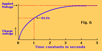
The capacitor slows down as it charges, and in actual fact never
reaches the full supply voltage. That being the case, the maximum charge it
receives in the timing circuit (66.6% of the supply voltage) is a little over
the charge received after a time constant
(63.2%).
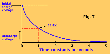
The capacitor slows down as
it discharges, and never quite reaches the ground potential. That means the
minimum voltage it operates at must be greater than zero. Timing circuit is
63.2% of the supply voltage.
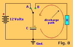
The discharge of a
capacitor also takes time and we can shorten the amount of time by decreasing
resistance (R) to the flow of
current.
Operating
Modes: The 555 timer has two basic operational modes: one shot and astable. In
the one-shot mode, the 555 acts like a monostable multivibrator. A monostable is
said to have a single stable state--that is the off state. Whenever it is
triggered by an input pulse, the monostable switches to its temporary state. It
remains in that state for a period of time determined by an RC network. It then
returns to its stable state. In other words, the monostable circuit generates a
single pulse of a fixed time duration each time it receives and input trigger
pulse. Thus the name one-shot. One-shot multivibrators are used for turning some
circuit or external component on or off for a specific length of time. It is
also used to generate delays. When multiple one-shots are cascaded, a variety of
sequential timing pulses can be generated. Those pulses will allow you to time
and sequence a number of related operations.
The other basic operational
mode of the 555 is as and astable multivibrator. An astable multivibrator is
simply and oscillator. The astable multivibrator generates a continuous stream
of rectangular off-on pulses that switch between two voltage levels. The
frequency of the pulses and their duty cycle are dependent upon the RC network
values.
One-Shot Operation: Fig. 4 shows the basic circuit of the 555
connected as a monostable multivibrator. An external RC network is connected
between the supply voltage and ground. The junction of the resistor and
capacitor is connected to the threshold input which is the input to the upper
comparator. The internal discharge transistor is also connected to the junction
of the resistor and the capacitor. An input trigger pulse is applied to the
trigger input, which is the input to the lower comparator.
With that
circuit configuration, the control flip-flop is initially reset. Therefore, the
output voltage is near zero volts. The signal from the control flip-flop causes
T1 to conduct and act as a short circuit across the external capacitor. For that
reason, the capacitor cannot charge. During that time, the input to the upper
comparator is near zero volts causing the comparator output to keep the control
flip-flop reset.
Notice how the monostable continues to output its pulse
regardless of the inputs swing back up. That is because the output is only
triggered by the input pulse, the output actually depends on the capacitor
charge.
Monostable Mode:
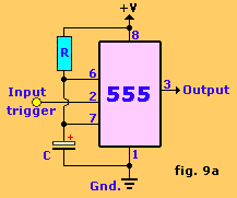
The 555 in fig. 9a is shown here in
it's utmost basic mode of operation; as a triggered monostable. One immediate
observation is the extreme simplicity of this circuit. Only two components to
make up a timer, a capacitor and a resistor. And for noise immunity maybe a
capacitor on pin 5. Due to the internal latching mechanism of the 555, the timer
will always time-out once triggered, regardless of any subsequent noise (such as
bounce) on the input trigger (pin 2). This is a great asset in interfacing the
555 with noisy sources. Just in case you don't know what 'bounce' is:
bounce is a type of fast, short term noise caused by a switch, relay, etc. and
then picked up by the input pin.
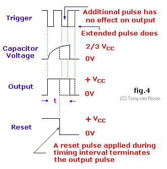
The trigger input is initially high (about
1/3 of +V). When a negative-going trigger pulse is applied to the trigger input
(see fig. 9a), the threshold on the lower comparator is exceeded. The lower
comparator, therefore, sets the flip-flop. That causes T1 to cut off, acting as
an open circuit. The setting of the flip-flop also causes a positive-going
output level which is the beginning of the output timing pulse.
The
capacitor now begins to charge through the external resistor. As soon as the
charge on the capacitor equal 2/3 of the supply voltage, the upper comparator
triggers and resets the control flip-flop. That terminates the output pulse
which switches back to zero. At this time, T1 again conducts thereby discharging
the capacitor. If a negative-going pulse is applied to the reset input while the
output pulse is high, it will be terminated immediately as that pulse will reset
the flip-flop.
Whenever a trigger pulse is applied to the input, the 555
will generate its single-duration output pulse. Depending upon the values of
external resistance and capacitance used, the output timing pulse may be
adjusted from approximately one millisecond to as high as on hundred seconds.
For time intervals less than approximately 1-millisecond, it is recommended that
standard logic one-shots designed for narrow pulses be used instead of a 555
timer. IC timers are normally used where long output pulses are required. In
this application, the duration of the output pulse in seconds is approximately
equal to:
T = 1.1 x R x C (in
seconds)
The output pulse width is defined by the above
formula and with relatively few restrictions, timing components R(t) and C(t)
can have a wide range of values. There is actually no theoretical upper limit on
T (output pulse width), only practical ones. The lower limit is 10uS. You may
consider the range of T to be 10uS to infinity, bounded only by R and C limits.
Special R(t) and C(t) techniques allow for timing periods of days, weeks, and
even months if so desired.
However, a reasonable lower limit for R(t) is in
the order of about 10Kilo ohm, mainly from the standpoint of power economy.
(Although R(t) can be lower that 10K without harm, there is no need for this
from the standpoint of achieving a short pulse width.) A practical minimum for
C(t) is about 95pF; below this the stray effects of capacitance become
noticeable, limiting accuracy and predictability. Since it is obvious that the
product of these two minimums yields a T that is less the 10uS, there is much
flexibility in the selection of R(t) and C(t). Usually C(t) is selected first to
minimize size (and expense); then R(t) is chosen.
The upper limit for
R(t) is in the order of about 15 Mega ohm but should be less than this if all
the accuracy of which the 555 is capable is to be achieved. The absolute upper
limit of R(t) is determined by the threshold current plus the discharge leakage
when the operating voltage is +5 volt. For example, with a threshold plus
leakage current of 120nA, this gives a maximum value of 14M for R(t) (very
optimistic value). Also, if the C(t) leakage current is such that the sum of the
threshold current and the leakage current is in excess of 120 nA the circuit
will never time-out because the upper threshold voltage will not be reached.
Therefore, it is good practice to select a value for R(t) so that, with a
voltage drop of 1/3 V+ across it, the value should be 100 times more, if
practical.
So, it should be obvious that the real limit to be placed on C(t)
is its leakage, not it's capacitance value, since larger-value capacitors have
higher leakages as a fact of life. Low-leakage types, like tantalum or NPO, are
available and preferred for long timing periods. Sometimes input trigger source
conditions can exist that will necessitate some type of signal conditioning to
ensure compatibility with the triggering requirements of the 555. This can be
achieved by adding another capacitor, one or two resistors and a small signal
diode to the input to form a pulse differentiator to shorten the input trigger
pulse to a width less than 10uS (in general, less than T). Their values and
criterion are not critical; the main one is that the width of the resulting
differentiated pulse (after C) should be less than the desired output
pulse for the period of time it is below the 1/3 V+ trigger level.
There
are several different types of 555 timers. The LM555 from National is the most
common one these days, in my opinion. The Exar XR-L555 timer is a micropower
version of the standard 555 offering a direct, pin-for-pin (also called
plug-compatible) substitute device with an advantage of a lower power operation.
It is capable of operation of a wider range of positive supply voltage from as
low as 2.7volt minimum up to 18 volts maximum. At a supply voltage of +5V, the
L555 will typically dissipate of about 900 microwatts, making it ideally
suitable for battery operated circuits. The internal schematic of the L555 is
very much similar to the standard 555 but with additional features like 'current
spiking' filtering, lower output drive capability, higher nodal impedances, and
better noise reduction system.
Maxim's ICM7555, and Sanyo's LC7555 models are a low-power, general
purpose CMOS design version of the standard 555, also with a direct pin-for-pin
compatibility with the regular 555. It's advantages are very low timing/bias
currents, low power-dissipation operation and an even wider voltage supply range
of as low as 2.0 volts to 18 volts. At 5 volts the 7555 will dissipate about 400
microwatts, making it also very suitable for battery operation. The internal
schematic of the 7555 (not shown) is however totally different from the normal
555 version because of the different design process with cmos technology. It has
much higher input impedances than the standard bipolar transistors used. The
cmos version removes essentially any timing component restraints related to
timer bias currents, allowing resistances as high as practical to be
used.
This very versatile version should be considered where a wide range of
timing is desired, as well as low power operation and low current sync'ing
appears to be important in the particular design.
A couple years after
Intersil, Texas Instruments came
on the market with another cmos variation called the LINCMOS (LINear CMOS) or
Turbo 555. In general, different manufacturers for the cmos 555's reduced the
current from 10mA to 100µA while the supply voltage minimum was reduced to about
2 volts, making it an ideal type for 3v applications. The cmos version is the
choice for battery powered circuits. However, the negative side for the cmos
555's is the reduced output current, both for sync and source, but this problem
can be solved by adding a amplifier transistor on the output if so required. For
comparison, the regular 555 can easily deliver a 200mA output versus 5 to 50mA
for the 7555. On the workbench the regular 555 reached a limited output
frequency of 180Khz while the 7555 easily surpassed the 1.1Mhz mark and the
TLC555 stopped at about 2.4Mhz. Components used were 1% Resistors and
low-leakage capacitors, supply voltage used was 10volt.
Some of the less
desirable properties of the regular 555 are high supply current, high trigger
current, double output transitions, and inability to run with very low supply
voltages. These problems have been remedied in a collection of CMOS
successors.
A caution about the regular 555 timer chips; the 555, along with
some other timer ic's, generates a big (about 150mA) supply current glitch
during each output transition. Be sure to use a hefty bypass capacitor over the
power connections near the timer chip. And even so, the 555 may have a tendency
to generate double output transitions.
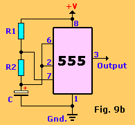 Astable operation: Figure 9b shows the 555 connected as an astable
multivibrator. Both the trigger and threshold inputs (pins 2 and 6) to the two
comparators are connected together and to the external capacitor. The capacitor
charges toward the supply voltage through the two resistors, R1 and R2. The
discharge pin (7) connected to the internal transistor is connected to the
junction of those two resistors.
Astable operation: Figure 9b shows the 555 connected as an astable
multivibrator. Both the trigger and threshold inputs (pins 2 and 6) to the two
comparators are connected together and to the external capacitor. The capacitor
charges toward the supply voltage through the two resistors, R1 and R2. The
discharge pin (7) connected to the internal transistor is connected to the
junction of those two resistors.
When power is first applied to the circuit,
the capacitor will be uncharged, therefore, both the trigger and threshold
inputs will be near zero volts (see Fig. 10). The lower comparator sets the
control flip-flop causing the output to switch high. That also turns off
transistor T1. That allows the capacitor to begin charging through R1 and R2. As
soon as the charge on the capacitor reaches 2/3 of the supply voltage, the upper
comparator will trigger causing the flip-flop to reset. That causes the output
to switch low. Transistor T1 also conducts. The effect of T1 conducting causes
resistor R2 to be connected across the external capacitor. Resistor R2 is
effectively connected to ground through internal transistor T1. The result of
that is that the capacitor now begins to discharge through R2.
The only
difference between the single 555, dual 556, and quad 558 (both 14-pin types),
is the common power rail. For the rest everything remains the same as the single
version, 8-pin 555.
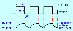 As soon as the voltage across
the capacitor reaches 1/3 of the supply voltage, the lower comparator is
triggered. That again causes the control flip-flop to set and the output to go
high. Transistor T1 cuts off and again the capacitor begins to charge. That
cycle continues to repeat with the capacitor alternately charging and
discharging, as the comparators cause the flip-flop to be repeatedly set and
reset. The resulting output is a continuous stream of rectangular
pulses.
As soon as the voltage across
the capacitor reaches 1/3 of the supply voltage, the lower comparator is
triggered. That again causes the control flip-flop to set and the output to go
high. Transistor T1 cuts off and again the capacitor begins to charge. That
cycle continues to repeat with the capacitor alternately charging and
discharging, as the comparators cause the flip-flop to be repeatedly set and
reset. The resulting output is a continuous stream of rectangular
pulses.
The frequency of operation of the astable circuit is dependent
upon the values of R1, R2, and C. The frequency can be calculated with the
formula:
f = 1/(.693 x C x (R1 + 2 x
R2))
The Frequency f is in Hz, R1 and R2 are in ohms, and C
is in farads. The time duration between pulses is known as the 'period', and
usually designated with a 't'. The pulse is on for t1 seconds, then off for t2
seconds. The total period (t) is t1 + t2 (see fig. 10). That time interval is
related to the frequency by the familiar relationship:
f = 1/t or t = 1/f
The
time intervals for the on and off portions of the output depend upon the values
of R1 and R2. The ratio of the time duration when the output pulse is high to
the total period is known as the duty-cycle. The duty-cycle can be calculated
with the formula:
D = t1/t = (R1 + R2) / (R1 +
2R2)
You can calculate t1 and t2 times with the formulas
below:
t1 = .693(R1+R2)C
t2 = .693 x R2 x C
The
555, when connected as shown in Fig. 9b, can produce duty-cycles in the range of
approximately 55 to 95%. A duty-cycle of 80% means that the output pulse is on
or high for 80% of the total period. The duty-cycle can be adjusted by varying
the values of R1 and R2.
Applications:
There are literally thousands of different
ways that the 555 can be used in electronic circuits. In almost every case,
however, the basic circuit is either a one-shot or an astable. The application
usually requires a specific pulse time duration, operation frequency, and
duty-cycle. Additional components may have to be connected to the 555 to
interface the device to external circuits or devices. In the remainder of this
experiment, you will build both the one-shot and astable circuits and learn
about some of the different kinds of applications that can be implemented.
Furthermore, the last page of this document contains 555 examples which you can
build and experiment with.
Required Parts:
In addition to a breadboard and a DC
powersupply with a voltage in the 5 to 12 volt range, you will need the
following components: 555 timer, LED, 2-inch /8 ohm loudspeaker, 150-ohm 1/4
watt resistor, two 10K ohm 1/4 resistors, two 1-Mega ohm 1/2 watt resistors, 10
Mega ohm 1/4 watt resistor, 0.1 µF capacitor, and a 0.68µF capacitor.
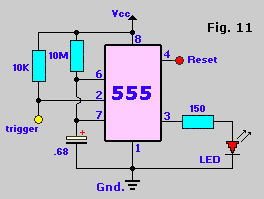 Experimental steps:
This circuit is resetable by grounding pin 4, so be
sure to have an extra wire at pin 4 ready to test that feature.
   1. On your breadboard, wire the one-shot circuit as shown in figure 11.

   2. Apply power to the circuit.  If you have a standard 5 volt logic supply,
       use it for convenience.  You may use any voltage between 5 and 15
       volts with a 555 timer. You can also run the circuit from battery power.
       A standard 9-volt battery will work perfectly.
       With the power connected, note the status of the LED:
            is it on or off? ________________

   3. Connect a short piece of hook-up wire to the trigger input line on pin 2.
       Momentarily, touch that wire to ground.  Remove it quickly.  That will
       create a pulse at the trigger input.
       Note and record the state of LED: _____________________

   4. Continue to observe the LED and note any change in the output state
       after a period of time.  What is the state? ______________

   5. When you trigger the one-shot, time the duration of the output pulse with
       a stopwatch or the seconds hand on your watch.  To do that, the instant
       that you trigger the one-shot by touching the wire to ground, immediately
       start your stopwatch or make note of the seconds hand on your watch.
       Trigger the one-shot and time the output pulse.  Write in the approximate
       value of the pulse-duration: ______________________

   6. Using the values of external resistor and capacitor values in Fig. 11 and
       the time interval formula for a one-shot, calculate the output-pulse duration.
              What is your value? _____________________

   7. Compare your calculated and timed values of output pulses.  Explain any
       discrepancies between your calculated and measured values.
             Answer: _________________________________________________

   8. Connect a short piece of hook-up wire  to pin 4.  You will use that as a
       reset.

   9. Trigger the one-shot as indicated previously.  Then immediately touch
       the reset wire from pin 4 to ground.  Note the LED result: _____________

 10. With a DC voltmeter, measure the output voltage at pin 3 during the one
      shot's off and on states.  What are your values?
           OFF: __________ volts         ON: ___________ volts.

 11. Replace the 10 MegOhm resistor with a 1 MegOhm resistor and repeat
      steps 5 and 6.  Record your timed and calculated results:
         Timed: ________ seconds         Calculated: _________seconds
If you want to get fancy, after you've completed the
experiment you can replace the resistors with potentiometers to build a variable
function generator and play with that to learn
more.
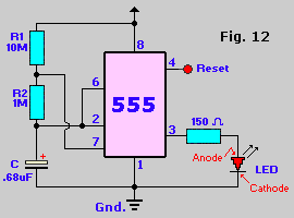
 12. Next you will experiment with astable circuits.  First, rewire the circuit so
      it appears as shown in Fig. 12.

 13. Apply power to the circuit and observe the LED.  What is happening?
      Answer: ____________________________________________________

 14. Replace the 10 MegOhm resistor with a 1 MegOhm resistor.  Again
      observe the LED.  Is the frequency higher or lower?  _________________

 15. Using the formula given in the tutorial, calculate the oscillation frequency
      using R1 as 10 MegOhm, and again with R1 as 1 MegOhm, and again with
      R1 as 10 MegOhm. R2 is 1 MegOhm in both cases.  Record your freq's:
               f = _____________ Hz  (R1 = 10 MegOhm)
               f = _____________ Hz  (R1 = 1 MegOhm)

 16. Calculate the period, t1 and t2, and the duty-cycle for each resistor value:
        10 MegOhm:  t = ___________  t1 = ____________  t2 = ____________

        1 MegOhm:   t = ___________  t1 = ____________  t2= ____________
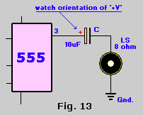
Monitoring the timer with a speaker can be
amusing if you switch capacitors or resistors to make an organ.
 17. Rewire the circuit making R1 and R2 10,000 ohms (10K) and C equal to 0.1µF.
      Use the same circuit in Fig. 12.  But, replace the LED and its resistor with
      a speaker and capacitor as shown in Fig. 13.

 18. Apply power to the circuit and note the result: ______________________

 19. Calculate the frequency of the circuit:  f = ____________________ Hz

 20. If you have an oscilloscope, monitor the output voltage on pin 3.
      Disconnect the speaker and note the output.  Also, observe the capacitor
      charge and discharge at pin 6 or 2: _____________________________
Review of steps 1 through 20:
The
circuit you built for those steps was a one-shot multi-vibrator. The circuit is
similar to that described in the tutorial. The trigger input is held high with a
10,000 ohm resistor. When you bring pin 2 low, by touching the wire to ground,
the one-shot is fired. The LED installed at the output of the 555 is used to
monitor the output pulse. The LED goes on when the one-shot is triggered.
The
component values selected for the circuit are large, so as to generate a long
output pulse. That allows you to measure the pulse duration with a stop watch.
Once the one-shot is triggered, the output LED stays on until the capacitor
charges to 2/3 of the supply voltage. That triggers the upper comparator and
causes the internal control flip-flop to reset, turning off the pulse and
discharging the capacitor. The one-shot will remain in that state until it is
triggered again.
Timing the pulse should have produced an output duration of
approximately 7.5 seconds. Calculating the output time interval using the
formula given previously, you found the pulse duration to be:
t = 1.1 x .68 x 10-6 x 107 = 7.48 seconds
You may have notice some difference between the calculated
and actual measured values. The differences probably result from inaccuracies in
your timing. Further more, component tolerances may be such that the actual
values are different from the marked values.
In steps 8 and 9 you
demonstrated the reset function. As you noticed, you could terminate the output
pulse before the timing cycle is completed by touching pin 4 to ground. That
instantly resets the flip-flop and shuts off the output pulse.
In step
10, you measured the output voltage. When off, the output is only a fraction
of a volt. For all practical purposes it is zero. When triggered, the 555
generates a 3.5 volt pulse with a 5-volt supply. If you used another value of
supply voltage, you would probably have discovered that the output during the
pulse is about 1.5 volt less than the supply voltage.
In step11, you
lowered the resistor value to 1 Megohm. As you noticed, that greatly shortens
the output pulse duration. The LED only stayed on for a brief time; so brief in
fact that you probably couldn't time it accurately. The calculated duration of
the output pulse is 0.748 seconds.
The circuit you built for steps 12 -
20 was an astable multi-vibrator. The astable circuit is an oscillator whose
frequency is dependent upon the R1, R2, and C values. In step 13, you
should have found that the LED flashed off and on slowly.
The oscillation
frequency is 0.176 Hz. That gives a period of:
t = 1/f = 1/.176 = 5.66
seconds
Since R1 is larger than R2, the LED will be on
for a little over 5 seconds and it will stay off for only 0.5 seconds.
That translates to a duty-cycle of:
D = t1/t = 5.18/5.66 = .915 or
91.5%
In step 14, you replaced the 10 MegOhm resistor
with a 1 MegOhm resistor making both R1 and R2 equal. The new frequency is 0.706
Hz, much higher than in step 13. That translates to a period of 1.41
seconds. Calculating the t1 and t2 times, you see that the LED is on for 0.942
second and off for 0.467 second. That represents a duty-cycle of:
D = 0.942/1.41 = 0.67 or
67%
In step 17, you made R1 = R2 = 10,000 ohm (10K)
and C = 0.1uF. That increased the frequency to 480Hz. The result should have
been a loud tone in the speaker.
If you had used an oscilloscope, you saw the
output to be a distorted rectangular wave of about 2 volts peak-to-peak. That
distortion is caused by the speaker load. Removing it makes the waveform nice
and square and the voltage rises to about 5 volts peak-to-peak. The capacitor
waveform is a combination of the classical charge and discharge curves given
earlier.
The time is useful in computer, function generators, clocks, music
synthesizers, games, flashing lights, printers, scanners and the list goes on
and on.
Example Circuits:
I have
placed a couple of 555 circuit examples below for your convenience. Play with
different component values and use the formulas mentioned earlier to calculate
your results. Things to remember: For proper monostable operation with the 555
timer, the negative-going trigger pulse width should be kept short compared tot
he desired output pulse width. Values for the external timing resistor and
capacitor can either be determined from the previous formulas. However, you
should stay within the ranges of resistances shown earlier to avoid the use of
large value electrolytic capacitors, since they tend to be leaky. Otherwise,
tantalum or mylar types should be used. (For noise immunity on most timer
circuits I recommend a 0.01uF (10nF) ceramic capacitor between pin 5 and
ground.) In all circuit diagrams below I used the LM555CN timer IC from
National, but the NE555 and others should not give you any problems.



Circuits 1 to
10a:
Play with different indicating devices such as bells,
horns, lights, relays, or whatever (if possible). Try different types of LDR's.
If for any reason you get false triggering, connect a ceramic 0.01uF (=10nF)
capacitor between pin 5 (555) and ground. Keeping the basic rules of the 555
timer, try different values for Ct and Rt (or the C & R over pins 2, 6 &
7) Replace Rt with a 1 megohm potentiometer if you wish. Make notes of the
values used and use the formulas to calculate timing. Verify your calculations
with your timing.
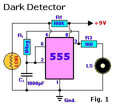
Fig. 1, Dark Detector:
It will sound an alarm if it gets too dark all over sudden. For
example, this circuit could be used to notify when a lamp (or bulb) burns out.
The detector used is a regular cadmium-sulphide Light Dependent Resistor or
LDR, for short, to sense the absence of light and to operate a
small speaker. The LDR enables the alarm when light falls below a certain
level.
Fig. 2, Power Alarm: This
circuit can be used as a audible 'Power-out Alarm'. It uses the 555 timer as an
oscillator biased off by the presence of line-based DC voltage. When the line
voltage fails, the bias is removed, and the tone will be heard in the speaker.
R1 and C1 provide the DC bias that charges capacitor Ct to over 2/3 voltage,
thereby holding the timer output low (as you learned previously). Diode D1
provides DC bias to the timer-supply pin and, optionally, charges a rechargeable
9-volt battery across D2. And when the line power fails, DC is furnished to the
timer through D2.
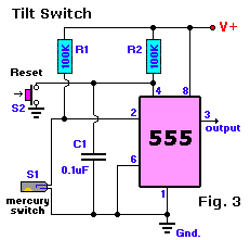
Fig. 3 Tilt Switch:
Actually really a alarm circuit, it shows how to use a 555 timer and
a small glass-encapsulated mercury switch to indicate 'tilt'.
The switch is
mounted in its normal 'open' position, which allows the timer output to stay
low, as established by C1 on startup. When S1 is disturbed, causing its contacts
to be bridged by the mercury blob, the 555 latch is set to a high output level
where it will stay even if the switch is returned to its starting position. The
high output can be used to enable an alarm of the visual or the audible type.
Switch S2 will silent the alarm and reset the latch. C1 is a ceramic 0.1uF (=100
nano-Farad) capacitor.
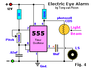
Fig. 4, Electric Eye
Alarm: The Electric-Eye Alarm is actually a similar circuit like the
Dark Detector of Fig. 1. The same type of LDR is used. The pitch for the speaker
can be set with the 500 kilo-ohm potentiometer. Watch for the orientation of the
positive (+) of the 10uF capacitor. The '+' goes to pin 3.
Fig. 5, Metronome: A Metronome is a device
used in the music industry. It indicates the rhythm by a 'toc-toc' sound which
speed can be adjusted with the 250K potentiometer. Very handy if you learning to
play music and need to keep the correct rhythm up.
Error fixed with thanks to
Grant Fair in regards to the two
resistors. (Grant also added a PNP power transistor to increase the volume and a
led for visual as well as sound output).
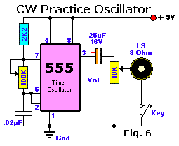
Fig. 6, CW Practice Oscillator: CW stands for
'Continuous Wave' or Morse-Code. You can practice the morse-code with
this circuit. The 100K potmeter is for the 'pitch' and the 10K for the speaker
volume. The "Key" is a morse code key.
Fig.
7, CW Monitor: This circuit monitors the morse code 'on-air' via the
tuning circuit hookup to pin 4 and the short wire antenna. The 100K potmeter
controls the tone-pitch.
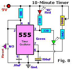
Fig. 8, Ten-Minute
Timer: Can be used as a time-out warning for Ham Radio. The Federal
Communications Commission (FCC) requires the ham radio operator to identify his
station by giving his call-sign at least every 10 minutes. This can be a
problem, especially during lengthy conversations when it is difficult to keep
track of time. The 555 is used as a one-shot so that a visual warning indicator
becomes active after 10-minutes. To begin the cycle, the reset switch is pressed
which causes the 'Green' led to light up. After 10 minutes, set by the
500K potentiometer R1, the 'Red' led will light to warn the operator that
he must identify.
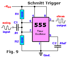
Fig. 9, Schmitt Trigger:
A very simple, but effective circuit. It cleans up any noisy input
signal in a nice, clean and square output signal. In radio control (R/C) it will
clean up noisy servo signals caused by rf interference by long servo leads. As
long as R1 equals R2, the 555 will automatically be biased for any supply
voltage in the 5 to 16 volt range. (Advanced Electronics: It should be noted
that there is a 180-degree phase shift.) This circuit also lends itself to
condition 60-Hz sine-wave reference signal taken from a 6.3 volt AC transformer
before driving a series of binary or divide-by-N counters. The major advantage
is that, unlike a conventional multivibrator type of squares which divides the
input frequency by 2, this method simply squares the 60-Hz sine wave reference
signal without division.
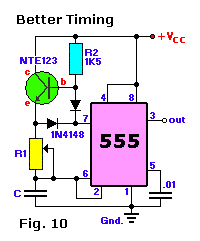
Fig. 10, Better
Timing: Better and more stable timing output is created with the
addition of a transistor and a diode to the R-C timing network. The frequency
can be varied over a wide range while maintaining a constant 50% duty-cycle.
When the output is high, the transistor is biased into saturation by R2
so that the charging current passes through the transistor and R1 to C. When the
output goes low, the discharge transistor (pin 7) cuts off the transistor
and discharges the capacitor through R1 and the diode. The high & low
periods are equal. The value of the capacitor (C) and the resistor (R1 or
potmeter) is not given. It is a mere example of how to do it and the values are
pending on the type of application, so choose your own values. The diode can be
any small signal diode like the NTE519, 1N4148, 1N914 or 1N3063, but a high
conductance Germanium or Schottky type for the diode will minimize the diode
voltage drops in the transistor and diode. However, the transistor should have a
high beta so that R2 can be large and still cause the transistor to saturate.
The transistor can be a TUN (europe), NTE123, 2N3569 and most
others.
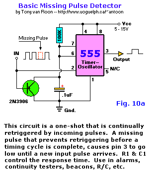
Fig. 10a, Missing Pulse Detector
(Basic): This transistor can be replaced with a ECG or NTE159. This
is just a basic model but works. Experiment with the values of Resistor and
Capacitor. A good example would be the 'Crashed Aircraft
Locator' beacon used in radio control. If there is no signal it sees it
as a missing pulse and sounds buzzer.
The following circuits are examples of how a 555 timer IC assist in
combination with another Integrated Circuit. Again, don't be
afraid to experiment. Unless you circumvent the min and max parameters of the
555, it is very hard to destroy. Just have fun and learn something doing it.

 Circuits 11 to 14:
Play with
different indicating devices such as bells, horns, lights, relays, or whatever
(if possible). Try different types of LDR's. If for any reason you get false
triggering, connect a ceramic 0.01uF (=10nF) capacitor between pin 5 (555) and
ground. In all circuit diagrams below I used the LM555CN timer IC from National.
The 555 timer will work with any voltage between 3.5 and 15volt. A 9-volt
battery is usually a general choice. Keeping notes is an important aspect of the
learning process.
Fig. 11, Two-Tones:
The purpose of this experiment is to wire two 555 timers together to
create a 2-note tone. If you wish, you can use the dual 556 timer
ic.
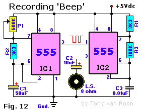
Fig. 12, Recording Beep:
This circuit is used to keep recording of telephone conversations
legal. As you may know, doing otherwise without consent of the other party is
illegal. The output of IC1 is fed to the 2nd 555's pin 3 and made audible via C2
and the speaker. Any 8-ohm speaker will do.
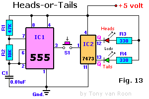
Fig. 13, Coin Toss: Electronic 'Heads-or-tails' coin toss
circuit. Basically a Yes or No decision maker when you can't make
up your mind yourself. The 555 is wired as a Astable Oscillator, driving in
turn, via pin 3, the 7473 flip-flop.
When you press S1 it randomly selects the 'Heads' or 'Tails' led. The leds
flashrate is about 2Khz (kilo-Hertz), which is much faster than your eyes can
follow, so initially it appears that both leds are 'ON'. As soon as the switch
is released only one led will be lit.
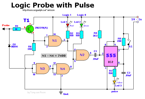
Fig.
14, Logic Probe: Provides you with three visible indicators; "Logic
1" (+, red led), "Logic 0" (-, green led), and "Pulse" (yellow led). Good for
TTL and CMOS. The yellow or 'pulse' led comes on for approximately 200 mSec to
indicate a pulse without regards to its width. This feature enables one to
observe a short-duration pulse that would otherwise not be seen on the logic 1
and 0 led's. A small switch (subminiature slide or momentary push) across the
20K resistor can be used to keep this "pulse" led on permanently after a pulse
occurs.
In operation, for a logic 0 input signal, both the '0' led and the
pulse led will come 'ON', but the 'pulse' led will go off after 200 mSec. The
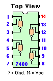
logic levels are detected via resistor R1 (1K), then amplified by T1 (NPN, Si-AF
Preamplifier/Driver), and selected by the 7400 IC for what they are. Diode D1 is
a small signal diode to protect the 7400
and the leds from excessive inverse voltages during capacitor discharge.
For
a logic '1' input, only the logic '1' led (red) will be 'ON'. With the switch
closed, the circuit will indicate whether a negative-going or positive-going
pulse has occurred. If the pulse is positive-going, both the '0' and 'pulse'
led's will be on. If the pulse is negative-going, the '1' and 'pulse' led's will
be on.
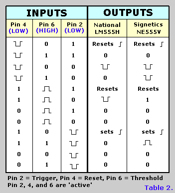
Check the listing in Table 2. It shows some
variations in the 555 manufacturing process by two different manufacturers,
National Semiconductor and Signetics Corporation. Since there are other
manufacturers then those two I suggest when you build a circuit to stick with
the particular 555 model they specify in the schematic.
Unless you know what
you're doing of course...
[grin].
The absolute maximum ratings (in free air) for NE/SA/SE types are:
                     Vcc, supply voltage: 18V
Input voltage (CONT, RESET, THRES, TRIG): Vcc
                          Output current: 225mA (approx)
          Operating free-air temp. range: NE555...........   0°C - 70°C
                                          SA555........... -40°C - 85°C
                                          SE555, SE555C... -55°C - 125°C
               Storage temperature range: -65°C - 150°C
Case temperature for 60sec. (FK package): 260°C
Suggested
Reading:
1. 555 Timer IC Circuits. Forrest
M. Mims III, Engineer's Mini Notebook. Radio Shack Cat. No: 62-5010.
"Create
& experiment with pulse generators, oscillators, and time delays."
2.
IC Timer Cookbook. Walter G. Jung. Published by Howard W. Sams & Co., Inc.
ISBN: 0-672-21932-8.
"A reference 'must' for hobby, technicians, and
engineers."
3. The 555 Timer Applications Sourcebook. Howard M. Berlin.
Published by Sams Inc. ISBN: 0-672-21538-1.
"Learn how to connect the 555,
perform 17 simple experiments."
Copyright © 1995 - Tony van Roon (VA3AVR).
ALL RIGHTS RESERVED.
Last updated:
September 8, 2005